
Applied Materials and Intel have announced a partnership to accelerate next-generation semiconductor innovation for AI...
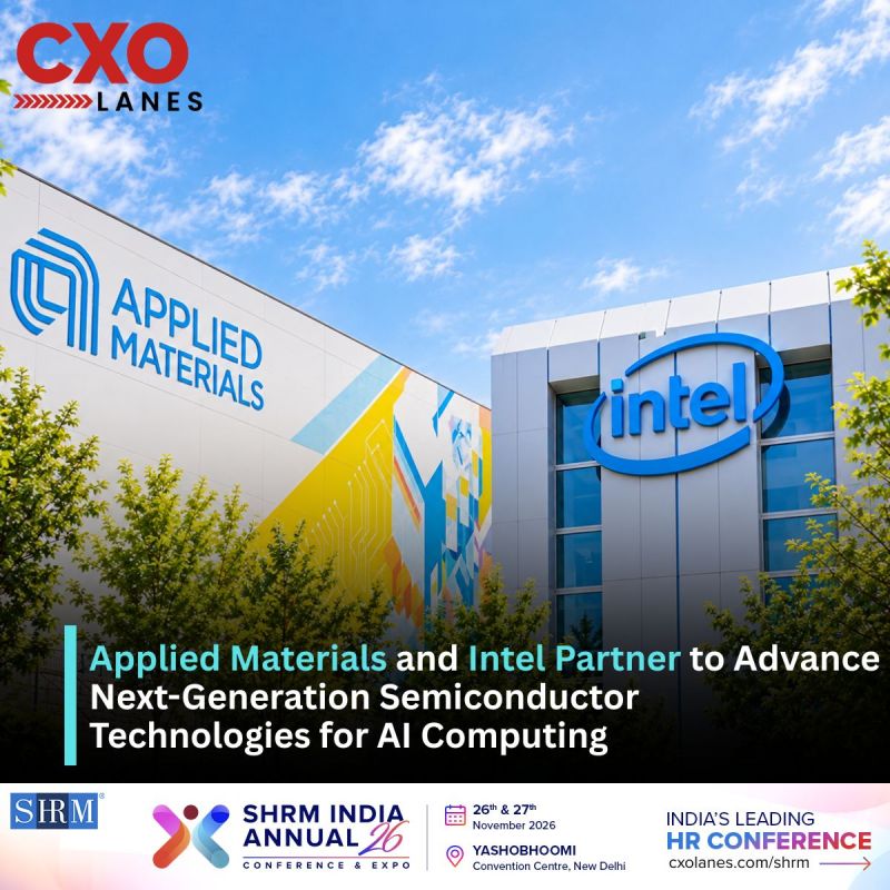
Applied Materials and Intel have announced a partnership to accelerate next-generation semiconductor innovation for AI computing. The collaboration will focus on advanced transistors, interconnects and packaging technologies to support increasingly demanding AI workloads, with research spanning Applied Materials’ EPIC Center in Silicon Valley and Intel’s R&D campus in Hillsboro, Oregon.
The partnership aims to develop new materials, manufacturing processes and device architectures for advanced logic nodes, including packaging technologies for Intel’s Foveros 3D chip-stacking platform. The initiative is designed to strengthen collaboration between research and manufacturing teams and accelerate the development of next-generation chip technologies.
Applied Materials CEO Gary Dickerson and Intel CEO Lip-Bu Tan highlighted the importance of closer collaboration in advancing semiconductor innovation. The companies aim to accelerate the transition from research to high-volume manufacturing in the United States as demand for AI computing infrastructure continues to grow.
Share this article
Send it to a colleague or post it to your network.